Antenna Design Interview Prep
Antenna design interview prep — radiation patterns, gain, directivity, VSWR, impedance matching, polarization, and MIMO antenna arrays.
Quick answer
Antenna design is the engineering discipline of converting bound currents on a structure into radiated electromagnetic waves (and vice versa) with target performance over a specified frequency band, polarization state, and angular pattern.
Antenna questions show up in RF, wireless, and product-engineering interviews because real-world link performance is gated by what the antenna does, not by what the modem can theoretically deliver.
Editorial review
Written by
CompoundLearn editorial team
Wireless / RF / hardware engineering
Reviewed by
CompoundLearn editorial team
Wireless / RF / hardware engineering
Last reviewed
Built from curated topic maps, editorial validation, and subject-matter review so the page stays aligned with the interview intent and the current content pipeline.
What it is
Antenna design is the engineering discipline of converting bound currents on a structure into radiated electromagnetic waves (and vice versa) with target performance over a specified frequency band, polarization state, and angular pattern. Core figures of merit include directivity (geometric concentration of radiated power in a chosen direction), efficiency (fraction of input power that is actually radiated rather than dissipated as heat), gain (the product of the two, in dBi), bandwidth (the band over which return loss and pattern stay within spec), VSWR / return loss (impedance match to the feedline), polarization (linear, circular, dual-pol), and beamwidth (half-power angular extent of the main lobe). Common topologies include the half-wave dipole, the printed patch (microstrip rectangular or circular, single- and dual-fed for circular polarization), the helix, the horn (high-gain, well-matched, large), the Yagi-Uda (directional, narrow band), the slot, and arrays of any of the above for MIMO and beamforming. Modern wireless system antennas are designed in 3D EM simulators (HFSS, CST, FEKO, Ansys, COMSOL) and validated in anechoic chambers; massive-MIMO arrays add calibration networks, mutual-coupling control, and active matching layers because hundreds of elements must behave as a coherent unit. Antenna design straddles RF, electromagnetics, mechanical packaging, and (for mobile devices) industrial design.
Why interviewers ask
Antenna questions show up in RF, wireless, and product-engineering interviews because real-world link performance is gated by what the antenna does, not by what the modem can theoretically deliver. Interviewers test whether a candidate can reason about figures of merit (gain versus directivity, why one is in the link budget and the other on the datasheet), about practical design tradeoffs (a patch with high gain but narrow bandwidth versus a helix with moderate gain but wide bandwidth and circular polarization), and about deployment realities (how nearby ground planes, dielectric loading, and human-body proximity de-tune a handheld antenna). A favorite interview probe is asking how you would design a 2.4-GHz / 5-GHz dual-band Wi-Fi antenna for a product the size of a USB stick — the answer requires reasoning about frequency-selective elements (PIFA arms, IFA traces), ground-plane size, and matching network compromises. MIMO antenna design questions probe envelope correlation, mutual coupling, and polarization diversity. Strong candidates connect each numerical specification to a measurable consequence: a VSWR of 3 wastes about 1.25 dB to mismatch, an envelope correlation coefficient of 0.7 cuts MIMO capacity, a 6-dB gain bump in the desired direction roughly doubles link range (range scales as the square root of gain). That quantitative grounding is what reviewers reward.
Common mistakes
Three common errors. First, conflating gain and directivity: candidates use them interchangeably, missing that efficiency separates the two and that low-efficiency designs (lossy substrate, narrow trace antennas in compact products, off-center feed) can have high directivity but mediocre gain. Second, treating VSWR as a single number: an antenna with VSWR 1.5 at center frequency but VSWR 4 at the band edge will fail the same link that a flatter VSWR 2 antenna passes; the band-wise specification matters. Third, ignoring near-field effects: a candidate who designs an antenna in isolation, ignoring nearby PCBs, batteries, metal cases, and human bodies, ships a product that performs nothing like the simulation. Adjacent traps include forgetting that ground-plane size strongly affects monopole and PIFA performance (a quarter-wave monopole on an undersized ground plane radiates very differently from one on an infinite plane), conflating polarization mismatch with antenna pattern misalignment (mismatch is a separate loss — about 3 dB for linear-to-circular, and ideally total for orthogonal linear or opposite-sense circular pairings, limited in practice to 20–30 dB by finite axial ratio and cross-pol purity), and assuming the manufacturer's datasheet pattern applies in your enclosure. Strong candidates flag the housing, the ground, the user, and the band edges as first-class design variables.
Sample interview questions
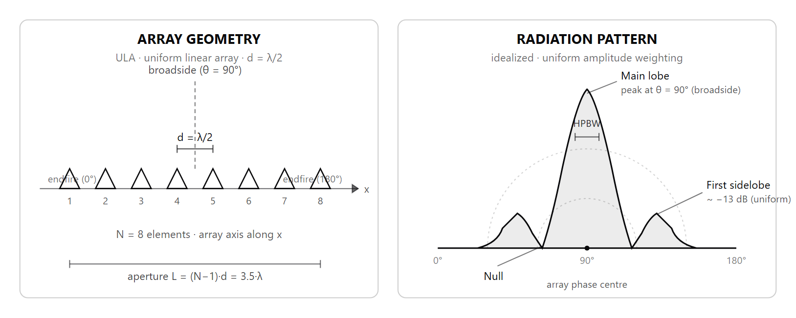
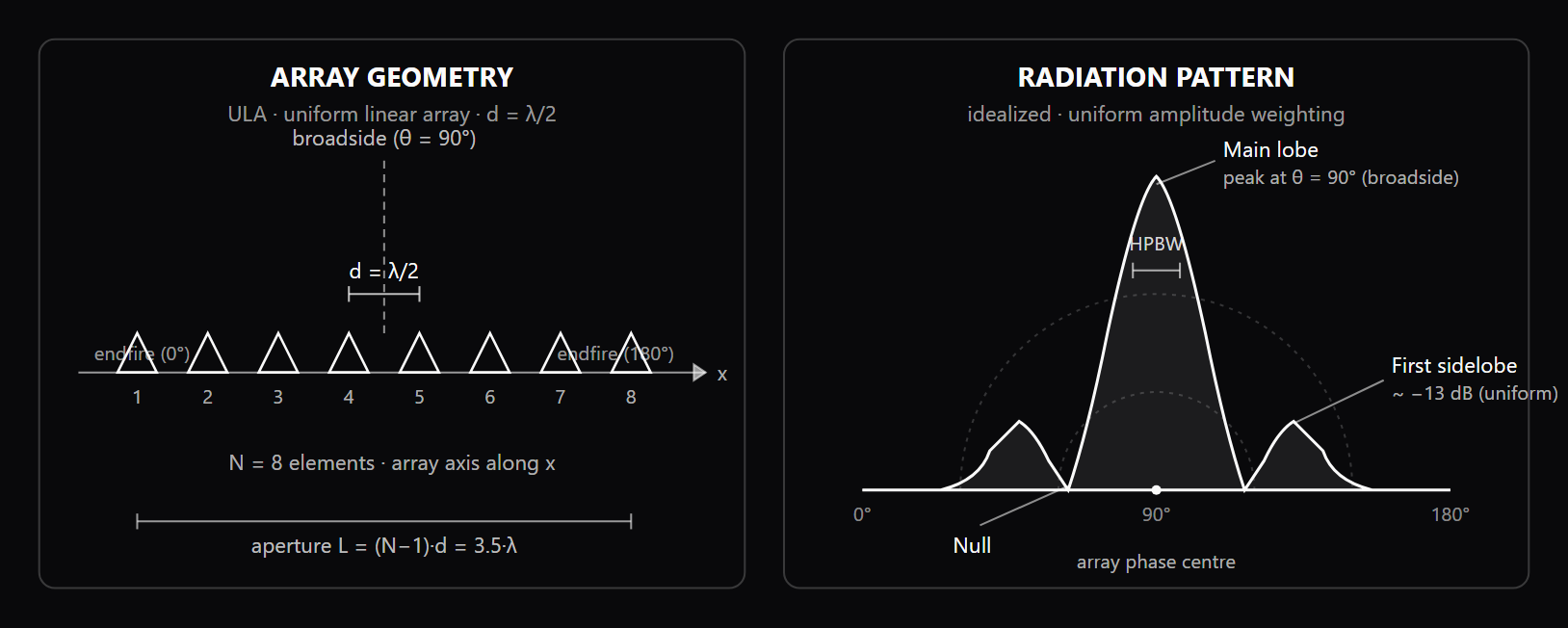
- In a uniform linear array intended to scan over a wide angular range, why is element spacing of d = λ/2 the canonical choice, and what fails when d exceeds λ/2?
- A. λ/2 spacing maximises mutual coupling between elements, which raises array gain proportionally and is the dominant array-design target.
- B. λ/2 spacing is the largest spacing that avoids visible grating lobes over near-hemispherical scan; for larger spacing, off-broadside steering can bring grating-lobe replicas of the main beam into the visible region. ✓
- C. λ/2 spacing is a manufacturing convention; spacing has no effect on the angular position of grating lobes in the visible region.
- D. λ/2 spacing minimises array aperture, so any deviation increases the physical footprint without changing the radiation pattern shape.
Option B is correct because the array factor of a uniform linear array repeats every 2π in electrical angle ψ = k·d·sinθ. With d = λ/2, the full range of physical scan angles θ ∈ [-90°, 90°] maps to ψ ∈ [-π, π], so the array factor only completes one period across the visible region and only the main beam appears. For d > λ/2 the same scan range maps to a wider ψ range, the array factor pattern repeats, and grating lobes (replicas of the main beam) enter the visible region at angles given by sin θ_g = sin θ_0 ± λ/d. At broadside (θ_0 = 0) and d = λ, grating lobes appear at ±90° (endfire). Below λ/2 the visible region underfills one period of the array factor — no grating lobes, but the array beamwidth narrows less per element added and mutual coupling intensifies, raising element-pattern distortion. Option A is incorrect because mutual coupling at λ/2 is moderate, not maximised, and coupling generally degrades — not raises — array gain by distorting the element pattern and shifting active impedance. Option C is incorrect because grating-lobe position is a geometric function of d, λ, and scan angle; it is governed by the array-factor equation, not by manufacturing convention. Option D is incorrect because aperture L = (N-1)d shrinks as d shrinks, but a smaller aperture widens the beam and lowers directivity — the radiation pattern shape changes substantially.
- A parabolic reflector lands aperture efficiency η_ap at 0.55-0.75. Which factor dominates the gap between effective and physical aperture?
- A. Illumination taper from the feed plus spillover past the rim — together they account for most of the 25-45% efficiency deficit; surface tolerance and blockage contribute the remainder. ✓
- B. Atmospheric absorption in the path between feed and reflector, which scales with frequency and is the dominant loss term at sub-6 GHz.
- C. The reflector is mismatched to free-space impedance, so half of the incident power is reflected back into the feed circuit.
- D. Polarization mismatch between the feed and the reflector surface, which is set by the substrate dielectric constant ε_r.
Option A is correct because aperture efficiency factors into roughly four multiplicative components: illumination efficiency η_i (the feed pattern weights the aperture non-uniformly, with edge-tapered illumination that radiates less than a uniform field), spillover efficiency η_s (energy from the feed that misses the reflector rim and radiates into the back hemisphere), surface-tolerance loss, commonly modeled by the Ruze factor exp[-(4πσ/λ)²] for RMS surface error σ, and blockage by the feed and support struts. Illumination and spillover are the two dominant terms; a feed designed to fully illuminate the reflector reduces spillover but accentuates the taper, and vice versa — the design point trades them. For a typical Cassegrain at 0.7 η_ap, illumination is around 0.85 and spillover around 0.85, multiplied with smaller surface and blockage factors. Option B is incorrect because atmospheric absorption is a propagation-channel effect external to the antenna; it does not enter the η_ap calculation, which compares effective collecting area to physical aperture area in vacuum. Option C is incorrect because a metal reflector at microwave is effectively a perfect electrical conductor; reflected power goes forward as the radiated beam, not back into the feed circuit. Option D is incorrect because the reflector surface itself does not impose a polarization; substrate ε_r is a printed-antenna parameter that does not apply to a metal parabolic dish.
- After impedance matching, an antenna shows VSWR ≈ 1.05 at band centre. Which conclusion about VSWR, S11, and radiation efficiency is correct?
- A. VSWR 1.05 means the feed reflection is very low at band centre, but this does not prove the antenna is radiating efficiently — ohmic and dielectric losses can dissipate the accepted power as heat. ✓
- B. A VSWR of 1:1 guarantees the antenna is radiating efficiently, and the 1.05 reading is essentially a perfect radiator across the entire VSWR bandwidth.
- C. Minimizing VSWR is the top design priority and overrides bandwidth, polarization, and pattern targets in every antenna optimisation.
- D. The VSWR bandwidth of an antenna equals its usable pattern bandwidth, so a flat VSWR plot proves the radiation pattern is also flat across the band.
Option A is correct because VSWR (and the related |S11|) only measures impedance match at the feed port: how much of the incident power is reflected back vs accepted into the antenna terminal. The remainder — the accepted power — is then split between radiated power and dissipated loss (ohmic in conductors, dielectric in substrate). A VSWR of 1.05 corresponds to about 0.003 dB of mismatch loss but says nothing about whether the accepted power radiates or heats the structure. A small lossy printed antenna can simultaneously have VSWR 1.05 and 30% radiation efficiency. Option B is incorrect because a VSWR of 1:1 guarantees the antenna is radiating efficiently is the KB-flagged false claim. VSWR is a match metric, not a radiation-efficiency metric. Option C is incorrect because Minimizing VSWR is always the top design priority is the KB-flagged false claim. In some designs (broadband or pattern-priority antennas) the engineer accepts a higher VSWR ceiling — e.g. VSWR 2.5 — across a wider band rather than VSWR 1.2 across a narrower band, because system performance is set by the joint impedance and pattern budget. Option D is incorrect because The VSWR bandwidth of an antenna equals its usable pattern bandwidth is the KB-flagged false claim. The impedance bandwidth and the pattern bandwidth are computed against different acceptance criteria and rarely coincide; many antennas show acceptable VSWR across a band over which the gain or polarization has already degraded.
- An 8×8 patch array shows higher edge-element VSWR than centre elements under scan. Which mutual-coupling statement is correct?
- A. Mutual coupling causes each element to see an active impedance that depends on the excitation of every other element, so VSWR shifts with scan angle and edge elements (fewer neighbours) experience a different active impedance than interior elements. ✓
- B. Mutual coupling is always detrimental to array performance, and it only occurs between elements that are directly adjacent in the array lattice.
- C. Increasing element spacing always reduces mutual coupling sufficiently to keep VSWR constant across scan, with no measurable change in array pattern.
- D. Mutual coupling affects only the radiation pattern; it has no effect on element impedance or VSWR seen at the array feed network.
Option A is correct because in a phased array the field at each element is the superposition of its own self-radiation plus coupled fields from every other element weighted by the array excitation. The result is an active (scan-dependent) input impedance Z_active = Z_self + Σ Z_mutual·(I_n/I_0), where the sum runs over neighbours and the excitation phases I_n change with scan angle. Edge elements see fewer coupled neighbours than interior elements, so their active impedance differs from the bulk and shifts more under scan — visible at the array feed as scan-angle-dependent VSWR variation. Option B is incorrect because Mutual coupling is always detrimental to array performance is the KB-flagged false claim. Coupling can be exploited — wideband electromagnetically-coupled arrays deliberately use strong coupling to extend impedance bandwidth. Option C is incorrect because Increasing element spacing always reduces mutual coupling sufficiently is the KB-flagged false claim. Coupling falls with spacing but never vanishes; meanwhile spacing greater than λ/2 introduces grating lobes (see question uS2uC1Xb), so the trade is not free. Option D is incorrect because mutual coupling changes both the active element pattern and the active input impedance, so it can shift the VSWR seen by the feed network as scan angle and excitation weights change.
- For a 28 GHz mmWave patch on a thin Rogers substrate, what is the dominant bandwidth constraint, and which substrate move trades against it?
- A. Patch bandwidth is set by substrate height h and ε_r: thicker substrate widens the impedance bandwidth but excites surface waves and degrades efficiency, so the design is a height-vs-surface-wave trade. ✓
- B. Patch antennas naturally have wide bandwidth, so substrate height is essentially a manufacturing choice with no effect on impedance bandwidth.
- C. Using a thicker substrate always improves patch antenna performance, with no penalty on radiation efficiency or surface-wave excitation.
- D. Patch antennas can only produce linear polarization, so substrate choice is constrained by the requirement to avoid circular polarization at 28 GHz.
Option A is correct because the impedance bandwidth of a half-wave patch on a grounded dielectric slab increases with substrate thickness h (relative to λ_0) and generally improves as the effective permittivity is lowered, while a denser/higher-ε_r substrate tends to narrow it. Thickening the substrate widens the impedance bandwidth but launches more power into substrate-bound surface waves that propagate parallel to the substrate, eventually scattering at the substrate edges and degrading the broadside efficiency. Designers cap h around 0.02-0.04 λ_0 at mmWave for this reason, and use stacked patches or aperture-coupled feeds to extend bandwidth beyond what a single thicker patch can reach. Option B is incorrect because Patch antennas naturally have wide bandwidth is the KB-flagged false claim. Basic patch antennas are narrowband (1-5%); wideband performance requires specific structural choices. Option C is incorrect because Using a thicker substrate always improves patch antenna performance is the KB-flagged false claim. Beyond a height threshold, surface-wave losses and feed-probe inductance degrade performance. Option D is incorrect because Patch antennas can only produce linear polarization is the KB-flagged false claim. Circular polarization is readily obtained with truncated-corner patches, dual-feed patches with 90° hybrid couplers, or single-feed patches with deliberate degenerate-mode splitting.
- A 16-element panel runs phased-array beamforming today; tomorrow software loads MIMO precoding on the same hardware. Which statement is correct?
- A. Phased-array and MIMO use the same physical array; the difference is the weight strategy — phased-array uses phase-only weights for a single steered beam, MIMO uses complex per-element weights from the channel matrix to send multiple spatial streams. ✓
- B. Phased-array scan loss is negligible at wide scan angles, so a 16-element array can steer to ±70° with no penalty in array gain or main-beam width.
- C. Adding more elements always proportionally narrows the main beam, with no contribution from element-pattern or array-factor coupling.
- D. Array factor is unaffected by mutual coupling between elements, so the radiation pattern is fully described by the array factor alone.
Option A is correct because the array is just a set of N antennas with controllable weights. Phased-array beamforming typically forms one steered beam with coordinated phase-only weights w_n = exp(j·k·n·d·sinθ_0) that align all element contributions in one direction θ_0 — single steered beam, no spatial multiplexing. MIMO precoding applies complex weights derived from the singular vectors of the channel matrix H, so the panel can send multiple independent spatial streams over the eigenmodes of H, trading single-beam gain for multi-stream capacity. The radiating aperture can be identical, but practical MIMO operation requires enough RF-chain/baseband access to support the intended stream count; what changes is whether the baseband processor computes phase-only steering weights or full complex precoding matrices. Option B is incorrect because Phased array scan loss is negligible at wide scan angles is the KB-flagged false claim. Scan loss is approximately 10·log10(cos θ_0) for a planar array (the projected aperture shrinks), reaching 3 dB at 60° and 4.6 dB at 70°. Option C is incorrect because Adding more elements always proportionally narrows the main beam is the KB-flagged false claim. Beamwidth narrows roughly as 1/N for uniform amplitude, but tapered amplitude weighting trades beam-width for sidelobe-level and breaks the strict 1/N scaling. Option D is incorrect because Array factor is unaffected by mutual coupling between elements is the KB-flagged false claim. Mutual coupling distorts the active element pattern; the total radiation pattern is the active element pattern multiplied by the array factor, and the active element pattern depends on coupling.
- A 120 GHz imaging system must achieve 50 dBi gain. Which architecture choice — reflector, phased array, or dielectric lens — wins, and why?
- A. A reflector wins on raw gain-per-cost at 120 GHz because aperture scales with diameter; phased arrays demand thousands of mmWave RF chains; lenses suffer reflection loss at the silicon-air interface and add weight per unit aperture. ✓
- B. A phased array wins because the array factor alone determines the total radiation pattern, so element-pattern and mutual-coupling effects can be ignored at this frequency.
- C. A silicon lens wins because the silicon lens has negligible reflection losses, so the only design parameter is the lens shape and any hemispherical form gives equivalent focusing.
- D. A reflector wins because at 120 GHz any antenna technology delivers 50 dBi with the same hardware budget and no architectural trade-off applies.
Option A is correct because gain G ≈ η_ap · 4π·A/λ². At 120 GHz (λ ≈ 2.5 mm) a 50 dBi target needs about 0.05 m² effective aperture, or about 0.083 m² physical aperture at η_ap = 0.6 — roughly a 32 cm reflector, which is cheap mechanically. A λ/2-spaced phased array would require tens of thousands of elements to deliver the same aperture — intractable cost and DC power at 120 GHz. A silicon lens of the same aperture is mechanically heavy (silicon density 2.33 g/cm³) and adds an air-to-silicon reflection at each interface unless anti-reflection layers are designed in. Reflector wins on raw gain-per-cost for fixed-pointing or slow-scan imaging. Option B is incorrect because The array factor alone determines the total radiation pattern is the KB-flagged false claim. The total pattern is the active element pattern times the array factor; element-pattern and mutual-coupling effects must be modelled, especially at mmWave where element directivity is substantial. Option C is incorrect because the silicon lens has negligible reflection losses is the KB-flagged false claim. The silicon-air interface has Fresnel reflection of about 30% per surface without anti-reflection coatings, and Any lens shape provides equivalent THz focusing is also wrong — extended hemispherical and elliptical geometries focus differently and only specific shapes minimise spherical aberration. Option D is incorrect because antenna technology choice at 120 GHz is dominated by cost, mass, scan flexibility, and tolerance — the trade-off is real and architectural.
Frequently asked questions
- What is the difference between gain, directivity, and efficiency?
- Directivity is a purely geometric property: the ratio of an antenna's radiation intensity in a specified direction to the average intensity over all directions, expressed in dBi (relative to an isotropic radiator). Radiation efficiency is the fraction of the power accepted by the antenna that is actually radiated, accounting for ohmic and dielectric losses (not impedance mismatch). Gain combines the two: gain = radiation efficiency * directivity. Folding in the impedance-mismatch loss as well gives realized gain — the figure the link budget ultimately cares about. A high-directivity antenna with poor efficiency (e.g., a tiny printed patch with a high-loss substrate) can have lower gain than a less directive antenna with better efficiency. Datasheets quote gain because that is what the link budget cares about; directivity matters for pattern shape; efficiency matters when you are debugging "why is my radiated power lower than my fed power."
- What does VSWR tell you about an antenna?
- Voltage Standing Wave Ratio measures the impedance match between the feedline and the antenna terminal: VSWR = (1 + |Gamma|) / (1 - |Gamma|), where Gamma is the reflection coefficient. A perfect match has VSWR = 1; common targets are VSWR < 2 (return loss > 9.5 dB) for general operation and < 1.5 (return loss > 14 dB) for tight specs. Bad VSWR matters for two reasons: power is reflected back into the PA where it can damage the device or trigger protection circuits, and the standing wave on the feedline causes additional cable loss. Always check VSWR over the full operating band — many antennas look great at center frequency and degrade near band edges. Sample question wW8yG7Zd drills into the VSWR vs radiation-efficiency distinction.
- How does antenna polarization affect link performance?
- Polarization describes the orientation of the electric-field vector. Linear polarization (vertical, horizontal, or slant) places the field along a fixed axis; circular polarization rotates the field at the wave frequency (left-hand or right-hand). Co-polarized antennas (both vertical, or both right-hand circular) couple efficiently. Cross-polarized antennas (vertical vs horizontal, RHCP vs LHCP) couple poorly — typically 20-30 dB of loss. Real systems exploit this for frequency reuse (orthogonal polarization on the same channel) or spatial multiplexing (dual-pol antennas with two independent streams). Polarization mismatch is also why a hand-held UE rotates around its axis without the link collapsing — pickup is reduced but not eliminated, and the channel's scatterers redistribute energy across polarizations.
- What is impedance matching and why is it critical?
- Maximum power transfer from a source to a load occurs when the load impedance is the complex conjugate of the source impedance. RF systems are usually 50-ohm (or 75-ohm in cable TV), so an antenna terminal that presents 50 + j0 ohms across the band is the ideal target. Real antennas drift in impedance as a function of frequency, so a matching network — discrete LC components, a microstrip stub, or a transformer — is added between feedline and antenna to bring the impedance into spec across the operating band. The match also has bandwidth limits (Bode-Fano theorem); narrow-band antennas are easy to match, ultra-wideband antennas require traveling-wave or self-similar geometries that present a stable impedance over decades.
- How are antenna arrays designed for MIMO operation?
- MIMO antenna arrays balance several constraints. Element spacing of about half a wavelength keeps mutual coupling tolerable and supports independent spatial dimensions; tighter spacing increases correlation and reduces effective rank. Polarization diversity (alternating slant +45 / -45 elements) doubles the antenna count for a given geometric footprint at the cost of a polarization-orthogonal channel pair. Pattern complementarity matters: each element should illuminate the cell as evenly as possible, with envelope correlation coefficients below 0.5 between any two ports across the band. For massive-MIMO arrays, additional concerns include calibration networks (a small RF feedback path that lets the BS measure each chain's response), grating-lobe suppression at scan angles, and thermal-balance design to keep the array linear as multiple PAs run simultaneously.
- What is the difference between array gain and antenna gain?
- These are three distinct numbers that interview candidates often conflate. Single-element gain G_e (dBi) is the directivity-times-efficiency of one antenna element — set by the element geometry (a dipole gives ~2.15 dBi, a microstrip patch ~6-8 dBi, a horn 10-20 dBi). Array factor gain G_af is the coherent combining gain from N elements driven with appropriate weights, which is 10·log10(N) for uniform amplitude and broadside steering (so 8 elements add 9 dB). Total array gain G_total ≈ G_e + G_af for a broadside-steered uniform array, derated for taper efficiency, mutual coupling, and scan angle. Amplitude tapers (Taylor, Chebyshev) trade array-factor gain for lower sidelobe levels; a heavily tapered array can lose 1-3 dB of G_af versus uniform amplitude in exchange for −30 dB sidelobes instead of −13 dB. The sample question uS2uC1Xb on λ/2 spacing and zC7eM9Cg on phased-array vs MIMO weight strategies both build on this decomposition.
- When is a circularly polarized antenna preferred over linear?
- Circular polarization (CP) is preferred in three deployment regimes. First, satellite communications: the polarization plane of a linearly polarized signal rotates as it transits the ionosphere (Faraday rotation) and the satellite-to-ground link geometry changes with the satellite pass, so a CP antenna receives both rotations without a 20-30 dB polarization-mismatch loss — GPS, Iridium, and most LEO/MEO terminals use CP. Second, mobile or hand-held terminals where the device orientation is unpredictable: a CP antenna pair (LHCP and RHCP) keeps the polarization-mismatch loss bounded to about 3 dB regardless of device tilt. Third, RFID and near-field imaging where the tag or target orientation is uncontrolled. CP is not magic, though: it costs an axial-ratio specification (real CP is elliptical, with axial ratios 1-3 dB), needs more complex feed networks (90° hybrids or truncated-corner patches), and only one of LHCP/RHCP couples to a CP receiver — picking the wrong sense gives the full polarization-loss penalty.
- How does a Yagi-Uda antenna achieve high directivity without active elements?
- A Yagi-Uda uses one driven dipole plus passive parasitic elements (one reflector behind the driven element, several directors in front) that re-radiate due to currents induced by the driven element. The reflector is slightly longer than the driven element and lags in phase, so its re-radiated field reinforces the driven element in the forward direction. Each director is slightly shorter than the driven element and leads in phase, pulling the radiation pattern forward. The whole structure works through mutual coupling — exactly the effect catalogued in sample question xY1aI3Ae — but turned into a design feature rather than a perturbation. Element spacing is typically 0.15-0.25 λ between reflector and driven element, 0.20-0.35 λ between directors, and directivity grows with boom length — a well-designed ~5λ Yagi reaches roughly 14-15 dBi, with diminishing returns (gain rises only about 1 dB per doubling of boom length once past a few λ). The geometry is narrowband (≈3-5% impedance bandwidth) and orientation-sensitive, which is why Yagi antennas dominate fixed-pointing applications (TV reception, point-to-point HF/VHF links) but not mobile devices.
Related topics
Pillar
Siblings
- Wireless Foundations
- Beamforming Interview Guide: Analog vs Digital vs Hybrid
- MIMO Explained: Spatial Multiplexing, Rank, Massive MIMO
- OFDM Explained: Subcarriers, Cyclic Prefix, PAPR, and OFDMA
- DSP Fundamentals
- Link Budget
- 5G NR Explained: Numerology, BWP, HARQ, and Frame Structure
- Electromagnetics
- RF Engineer Interview Signals
Practice
Essential AI-Native Skills for Antenna Design
Modern engineering work increasingly uses AI tools for design and code review, debugging, documentation, test and testbench generation, and workflow automation. The goal is not to let AI replace engineering judgment — it is to move faster while keeping verification discipline.
- Use AI to explain unfamiliar code, logs, waveforms, datasheets, or test failures.
- Break large problems into small, reviewable steps you can verify independently.
- Ask AI for hypotheses, then validate them against tests, measurements, simulations, or lab data.
- Version-control your analysis scripts, testbenches, and configs — keep changes small and reviewable.
- Document your assumptions, design tradeoffs, and debugging decisions.
- Verify AI output before trusting it: run the checks that fit the domain — unit tests, linters, simulations, or bench/lab measurements.
- Review AI output for correctness, edge cases, and real-world consequences.
Antenna Design — coming to the question bank
The adaptive practice engine is already live for core wireless, RF, and ML systems. Antenna Design isn't covered in the question bank yet — get notified when it's added.