Silicon Photonics for Datacenters Explained: 800G+ Links Interview Prep
Silicon photonics for datacenters explained: CMOS-compatible modulators, waveguides, and dense integration enabling 800G/1.6T pluggable, coherent, and co-packaged optical engines.
Quick answer
Silicon photonics (SiPh) integrates optical functions — waveguides, modulators, photodetectors, multiplexers — on silicon chips using CMOS-compatible fabrication processes.
Silicon photonics is the deep-physics + cost-economics question in optical-transceiver interviews.
Editorial review
Written by
CompoundLearn editorial team
Wireless / RF / hardware engineering
Reviewed by
CompoundLearn editorial team
Wireless / RF / hardware engineering
Last reviewed
Built from curated topic maps, editorial validation, and subject-matter review so the page stays aligned with the interview intent and the current content pipeline.
What it is
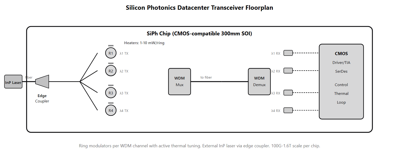
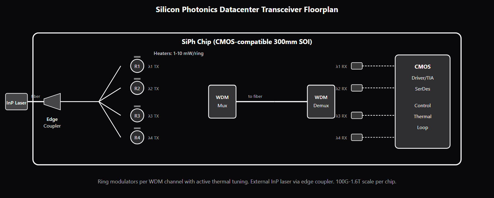
Silicon photonics (SiPh) integrates optical functions — waveguides, modulators, photodetectors, multiplexers — on silicon chips using CMOS-compatible fabrication processes. SiPh dominates short-reach datacenter optics (intra-datacenter 100m-2km links at 100G through 800G+) because the CMOS-compatible fab delivers economies of scale that InP and III-V platforms cannot match at volume. SiPh is also the foundation for CPO (co-packaged optics, see /topics/cpo-vs-pluggable-optics) in next-generation AI cluster networks where transceiver density and power per bit are binding constraints. The CMOS-compatible advantage is the central economic argument. SiPh devices use 300mm silicon wafers, the same process tools and materials as standard CMOS chips. This delivers shared fab capacity, mature process control, and supply-chain resilience that specialized photonics fabs cannot match. The trade-off vs III-V platforms (InP, GaAs) is silicon's indirect bandgap — silicon cannot efficiently lase, requiring external laser sources or III-V integration (hybrid bonding or heterogeneous epitaxy). Ring modulators are the core SiPh modulator. A microring resonator (10-50 μm diameter) modulates the optical carrier by tuning the resonance frequency in response to applied voltage via the plasma-dispersion effect. At resonance, light couples into the ring and is dropped; off-resonance, light passes through. Ring modulators are very compact and sub-pJ/bit at GHz rates, but bandwidth-limited (resonance Q) and thermally sensitive — silicon's thermo-optic coefficient (1.8×10⁻⁴ /°C) means the resonance shifts 75-100 pm/°C, requiring active thermal stabilization. Each ring needs an integrated heater plus closed-loop feedback from a monitor photodiode, consuming 1-10 mW per ring. In a 16-channel transceiver, thermal tuning is 80-160 mW just for stabilization — significant in the per-channel power budget. Mach-Zehnder modulators (see /topics/mach-zehnder-modulators-and-vpi) are the alternative SiPh modulator. They are broadband, not thermally sensitive, but larger (mm-class) and higher V_π. The SiPh-vs-MZM trade-off: rings win for compact dense-WDM datacenter applications where size and per-bit power matter; MZMs win for broadband coherent and longer-reach applications where thermal sensitivity is unacceptable. Edge couplers and grating couplers handle the optical I/O between the SiPh chip and external fiber. Edge couplers taper from the silicon waveguide mode to the fiber mode through a graded-width taper; production insertion loss typically 0.5-2 dB. Grating couplers use periodic grating structures to couple vertically from a fiber pointed at the chip surface; 1-3 dB insertion loss, polarization-sensitive, but easier to align and useful for wafer-level testing. Production SiPh transceivers usually use edge couplers; research and wafer-level test use grating couplers. Fiber-attach is the production process of bonding fiber pigtails to the SiPh chip edge couplers with sub-micron alignment precision. Approaches include passive alignment (mechanical features guide positioning), active alignment (per-unit tuning with laser feedback), and V-groove attachment (silicon V-grooves provide passive fiber positioning). Fiber-attach is 10-20% of total transceiver assembly cost and one of the dominant yield-limiters. On-chip lasers remain the hardest SiPh integration challenge. Three approaches: hybrid bonding (mature, Intel and Ayar Labs use it), heterogeneous epitaxy (research-stage, promising), and external laser sources (dominant production approach, simple but adds optical-coupling complexity). The choice affects per-channel cost, power consumption, reliability, and chip count. SiPh deployments in 2026 span 100G/200G/400G/800G+ datacenter optics (typically PAM-4 or PAM-6 direct-detection for short reach, coherent for longer reach), 400ZR/800ZR coherent pluggables (with InP lasers integrated externally), and emerging CPO architectures for AI cluster networks. The high-bandwidth high-density AI-cluster workload is pushing SiPh from per-server pluggables toward per-die CPO integration.
Why interviewers ask
Silicon photonics is the deep-physics + cost-economics question in optical-transceiver interviews. A candidate who fluently navigates SiPh's CMOS-compatible advantage, ring-modulator design trade-offs, thermal tuning, edge-coupler vs grating-coupler choices, and the InP-integration question for lasers is showing the integrated-device understanding that staff SiPh-design and transceiver-architect roles require. The CMOS-compatible economic argument is the diagnostic question. Strong candidates explain that SiPh's cost advantage at volume comes from shared 300mm fab capacity with CPU/memory production, and that this is what positions SiPh against InP for high-volume datacenter applications. Weak candidates know SiPh is CMOS-related but cannot articulate the economic dynamic. Thermal tuning is the operational-design probe. Strong candidates know silicon's thermo-optic coefficient and the resulting resonance-shift-per-°C, explain that integrated heaters with closed-loop feedback are the standard mitigation, and quote the per-ring power penalty (1-10 mW). They connect this to the per-channel power budget in dense transceivers. The on-chip-laser question is the integration-strategy probe. Strong candidates explain silicon's indirect bandgap as the fundamental constraint, name the three integration approaches (hybrid bonding, heterogeneous epitaxy, external laser), and identify the dominant production approach. They understand this is still an active research-to-production transition area. Ring-modulator vs MZM is the modulator-choice probe. Strong candidates explain that rings win for compact dense-WDM with thermal stabilization, MZMs win for broadband and longer-reach where size matters less. They name the bandwidth, power, and thermal-sensitivity trade-offs. The CPO integration question is the forward-looking probe. Strong candidates connect SiPh to CPO (next-generation AI cluster networks), explain why SiPh is the natural CPO substrate (CMOS-compatible, can be co-packaged with the host ASIC), and identify the binding constraints (power per bit, thermal budget, optical I/O density). See /topics/cpo-vs-pluggable-optics for the deeper CPO context.
Common mistakes
The most common mistake is treating silicon photonics as just "small optical chip." The CMOS-compatible economic argument is the defining feature — it positions SiPh against InP/GaAs platforms for high-volume datacenter applications. Candidates who do not surface the cost-at-scale dynamic miss the central platform argument. A second gap is missing thermal tuning. Silicon's thermo-optic coefficient is large enough that ring modulators need active thermal stabilization — without it, a 10°C temperature change can detune the ring entirely out of its WDM channel. Candidates who do not know thermal tuning is required, or who do not quote per-ring power consumption, have not worked at the SiPh device-design level. A third gap is collapsing edge couplers and grating couplers. They are different optical-I/O approaches with different alignment tolerances, polarization handling, and insertion-loss characteristics. Edge couplers dominate production; grating couplers are common in research and wafer-test. Candidates who treat them as interchangeable miss real engineering trade-offs. A fourth gap is missing the on-chip-laser challenge. Silicon's indirect bandgap is the fundamental constraint that drives all of SiPh's laser-integration architectures. Candidates who claim "silicon lasers work fine" misunderstand basic semiconductor physics; candidates who say "lasers don't matter in SiPh" miss that every transceiver needs at least one laser somewhere. A fifth gap is treating SiPh and InP as interchangeable. They are different platforms with different strengths. SiPh dominates volume short-reach datacenter; InP dominates very-high-speed coherent and on-chip-laser applications. Candidates who pick one as universally better miss the application-specific dynamic. See /topics/mach-zehnder-modulators-and-vpi for the MZM-side modulator detail, /topics/cpo-vs-pluggable-optics for the CPO deployment context, and /topics/coherent-optical-detection for the coherent-transceiver context that increasingly uses SiPh.
Silicon Photonics vs InP vs LN — Datacenter Optics
| Platform | Strengths | Limitations | Best Application |
|---|---|---|---|
| Silicon Photonics (SiPh) | CMOS-compatible fab, cost at scale, compact ring modulators | No on-chip laser, thermal-tuning power | 100G-800G datacenter, CPO, coherent pluggables |
| Indium Phosphide (InP) | On-chip lasers, very high bandwidth, mature for coherent | Higher cost, smaller wafers, less scalable | Very high-speed coherent, on-chip-laser apps |
| Lithium Niobate (TFLN) | Lowest V_π·L, excellent modulator linearity | No active devices, separate platform integration | Long-reach coherent transmitters |
Sample interview questions
- A silicon-photonics ring modulator drifts in resonance frequency by ~10 pm/°C. Why is thermal tuning a critical design concern, and what compensation strategies are used?
- A. Thermal effects are negligible in silicon photonics.
- B. Silicon's thermo-optic coefficient (dn/dT ≈ 1.8×10⁻⁴ /°C) means a ring modulator's resonance wavelength shifts by ~75-100 pm/°C — orders of magnitude larger than the modulator's 3-dB bandwidth. Without compensation, a 10°C temperature change would detune the ring out of the WDM channel. Compensation: integrated heater per ring (active thermal tuning with closed-loop feedback from a monitor photodiode), thermo-optic athermalization (negative-coefficient polymer cladding to cancel the silicon coefficient), or wavelength-agnostic operation (use Mach-Zehnder instead of ring). Active thermal tuning is the dominant approach but consumes 1-10 mW per ring — significant in a 16-channel datacenter transceiver. ✓
- C. Silicon photonics operates only at cryogenic temperatures.
- D. Thermal tuning is the same problem as PMD in fiber.
Option B is correct. Silicon's thermo-optic coefficient is ~1.8×10⁻⁴ per °C — the refractive index changes meaningfully with temperature. For a ring modulator with FSR (free spectral range) of ~10 nm and a 3-dB bandwidth of ~10-30 GHz (~0.08-0.24 nm), the resonance shifts ~75-100 pm/°C, which is comparable to or larger than the bandwidth itself. A 10°C temperature change can shift the ring entirely out of the target WDM channel. Compensation approaches: - **Active thermal tuning**: integrated TiN or polysilicon heaters wrap each ring, controlled by closed-loop feedback from a monitor photodiode that detects the through-port intensity. The controller adjusts heater current to lock the ring on the laser wavelength. Adds 1-10 mW per ring per channel — significant in a 16-channel transceiver (~80-160 mW just for thermal stabilization). - **Thermo-optic athermalization**: pair the silicon waveguide with a polymer cladding having negative dn/dT. The combined system has near-zero net coefficient. Reduces tuning power but adds fabrication complexity. - **Wavelength-agnostic modulators**: Mach-Zehnder modulators (see /topics/mach-zehnder-modulators-and-vpi) are not resonance-based and avoid thermal sensitivity, at the cost of larger footprint and higher V_π. - **Operating temperature stabilization**: place the SiPh chip on a thermoelectric cooler (TEC) — uses bulk power but stabilizes the whole chip rather than per-ring. The thermal-tuning power budget is one of the binding constraints on silicon-photonics transceiver design. CPO architectures (see /topics/cpo-vs-pluggable-optics) must include thermal tuning in the per-port power budget that the host ASIC delivers. Option A misses the dominant SiPh design concern. Option C is wrong — silicon photonics operates at standard temperatures. Option D confuses unrelated phenomena.
- Why is the integration of high-performance lasers directly on silicon photonics chips still considered challenging?
- A. Silicon's indirect bandgap makes it a poor light emitter — silicon cannot efficiently lase. III-V materials (InP, GaAs) lase efficiently because of their direct bandgaps. Integrating III-V lasers on silicon requires either hybrid bonding (wafer-bond III-V die on top of silicon), heterogeneous epitaxy (grow III-V on silicon with buffer layers for lattice-mismatch), or external laser sources (off-chip InP laser coupled via edge coupler). Each has trade-offs. The current production approach is mostly external-laser plus edge-coupler integration; integrated lasers are still primarily research-stage. ✓
- B. Lasers can be easily integrated; this is a solved problem.
- C. Silicon photonics does not need lasers.
- D. Lasers require electrical power that silicon cannot supply.
Option A is correct. Silicon has an indirect bandgap, meaning electron-hole recombination requires phonon assistance — the radiative efficiency is too low for practical laser operation. III-V semiconductors (InP, GaAs, GaN) have direct bandgaps where recombination is radiative without phonon mediation, enabling efficient lasing. This fundamental physical limitation is the reason silicon photonics needs III-V integration for on-chip lasers, and why the field has spent two decades on integration approaches: **Hybrid bonding**: III-V die is wafer-bonded onto a silicon photonics wafer post-fabrication. The III-V provides the gain medium; silicon waveguides route the light. Mature approach (Intel's integrated photonics roadmap, Ayar Labs SuperNova) but adds bonding complexity and per-die alignment tolerance. **Heterogeneous epitaxy**: III-V grown directly on silicon with thick buffer layers (typically 2-10 μm of intermediate material) to absorb lattice-mismatch dislocations. Promising research but yield and reliability for production are still maturing. **External laser source**: separate InP laser package coupled to the SiPh chip via edge coupler. Simplest integration but loses some of SiPh's "all-on-chip" appeal. Current dominant production approach for SiPh transceivers. **Quantum-dot lasers on silicon**: emerging research direction using QD active region tolerant of lattice mismatch. Pre-commercial as of 2026. The integration choice affects: per-channel cost (external laser adds optical-coupling complexity), power consumption (heterogeneous typically more efficient), reliability (external is most mature), and silicon-photonics chip count (hybrid/heterogeneous reduce chip count). Why this matters for datacenter optics: each transceiver needs one or more laser sources at specific wavelengths (typically the O-band 1310 nm for short-reach datacenter, or DWDM C-band wavelengths for longer reach). Laser cost can dominate per-transceiver BOM if integration is poor. Option B oversimplifies a still-active research area. Option C is wrong — silicon photonics absolutely needs lasers. Option D inverts the issue.
Frequently asked questions
- What is silicon photonics?
- Silicon photonics (SiPh) is the platform that integrates optical functions (waveguides, modulators, photodetectors, multiplexers) on silicon chips fabricated using CMOS-compatible processes. The CMOS-compatible fab is the key economic advantage — SiPh leverages existing semiconductor manufacturing infrastructure for volume production at low per-chip cost. Silicon photonics dominates short-reach datacenter optics (intra-datacenter 100m-2km links at 100G/200G/400G/800G+), is increasingly used in coherent transceivers (400ZR pluggables), and is the foundation for CPO (co-packaged optics) in next-generation AI cluster networks.
- Why is silicon photonics CMOS-compatible fabrication important?
- CMOS-compatible fabrication means SiPh devices use the same process tools, materials, and wafers (300 mm silicon) as standard CMOS chip manufacturing. This delivers: (1) economies of scale from sharing fab capacity with CPU/memory production; (2) maturity — SiPh inherits decades of CMOS process development; (3) integration potential — SiPh and CMOS can be fabricated together on the same wafer (or assembled at the same foundry); (4) supply-chain resilience — SiPh production is not dependent on specialized photonics fabs. The trade-off vs III-V platforms (InP, GaAs): silicon's indirect bandgap means it cannot efficiently lase, requiring external laser sources or III-V integration. The economic advantage outweighs the laser-integration challenge for most volume applications.
- What is a ring modulator and how does it work?
- A ring modulator is a SiPh device that modulates an optical carrier by tuning a microring resonator's resonance frequency in response to applied electrical voltage. At resonance, light couples into the ring and is dropped from the through-port (modulated off-state). Off-resonance, light passes through the through-port (on-state). Applied voltage shifts the resonance via the plasma-dispersion effect (carrier injection/depletion changes the refractive index). Ring modulators are very compact (10-50 μm diameter), very low-power per bit (sub-pJ/bit at GHz modulation rates), and CMOS-compatible. The trade-offs: narrow operating bandwidth (resonance Q), thermal sensitivity (resonance shifts ~75-100 pm/°C requiring active thermal stabilization), and wavelength-specific operation (each ring is designed for one carrier wavelength).
- What is an edge coupler vs grating coupler?
- Edge coupler: light enters/exits the SiPh chip through the chip edge (cleaved or polished facet). The waveguide tapers from the silicon dimension (sub-micron) to a larger mode-field matched to the external fiber. Insertion loss typically 0.5-2 dB. Polarization-insensitive in well-designed structures. Used for production SiPh transceivers. Grating coupler: a periodic grating on the chip surface couples light vertically from a fiber pointed at the chip. Insertion loss typically 1-3 dB per coupler. Polarization-sensitive (typically one polarization at a time, requiring a polarization-diversity scheme for full-pol systems). Easier to align (vertical coupling tolerates lateral offset). Used heavily in research and wafer-level testing; some production uses. The choice depends on production volume (edge coupler easier to scale), wafer-test needs (grating coupler enables non-destructive wafer probe), and polarization handling.
- What is fiber-attach in silicon photonics?
- Fiber-attach is the production process of bonding optical fibers to the SiPh chip's edge couplers (or grating couplers) with sub-micron alignment precision. Sub-micron alignment is required because the silicon waveguide mode is ~1 μm and lateral misalignment of 0.5 μm can cause significant insertion loss. The fiber pigtail provides the optical I/O to the outside world. Production fiber-attach approaches include passive alignment (mechanical features guide the fiber to position, no per-unit active tuning), active alignment (per-unit alignment optimization using a laser feedback signal), and V-groove attachment (silicon V-grooves etched in the chip provide passive fiber positioning). Fiber-attach is a non-trivial part of SiPh transceiver cost and yield — typically 10-20% of total transceiver assembly cost.
- How does thermal tuning work in silicon-photonics rings?
- Silicon's thermo-optic coefficient is ~1.8×10⁻⁴ per °C — a ring modulator's resonance wavelength shifts ~75-100 pm/°C. To maintain operation on a fixed WDM channel, each ring needs active thermal stabilization. Implementation: TiN or polysilicon heater wrapped around each ring, integrated photodiode monitoring the through-port intensity, closed-loop controller adjusts heater current to maintain the target resonance frequency. Power consumption: 1-10 mW per ring depending on design. In a 16-channel transceiver with one ring per channel, thermal tuning consumes 80-160 mW — significant in the per-channel power budget. Athermalization approaches (negative-coefficient polymer cladding to cancel silicon's coefficient) reduce tuning power at the cost of fabrication complexity.
- Why does silicon photonics struggle with on-chip lasers?
- Silicon has an indirect bandgap — electron-hole recombination requires phonon assistance, making radiative efficiency too low for practical lasing. III-V semiconductors (InP, GaAs, GaN) have direct bandgaps and lase efficiently. SiPh approaches to overcome this: hybrid bonding (wafer-bond III-V die on silicon), heterogeneous epitaxy (grow III-V on silicon through buffer layers), or external laser sources (off-chip InP laser coupled via edge coupler). The dominant production approach is external-laser-plus-edge-coupler; integrated lasers via bonding are commercial in select Intel and Ayar Labs products; heterogeneous epitaxy is mostly research. The integration choice affects per-channel cost, power consumption, and reliability. The economic question — does the integrated-laser option cost less than the external option at volume — determines which approach wins per generation.
- When does silicon photonics beat InP?
- Silicon photonics beats InP for high-volume short-reach datacenter applications where the cost advantage of CMOS-compatible fab dominates. SiPh production cost at scale is 30-70% lower than equivalent InP, primarily from shared 300mm CMOS fab capacity. For 100G/200G/400G/800G+ datacenter optics serving thousands of transceivers per cluster, SiPh is the cost-winning platform. InP beats SiPh when: (a) on-chip lasers are required and external sources are impractical (some embedded applications), (b) extreme bandwidth is needed (InP modulators reach higher speeds at moderate V_π·L), (c) volume is small (the SiPh scale advantage requires high volume to materialize), or (d) wavelength outside SiPh's well-developed bands. The current production split: SiPh dominates 100G+ datacenter optics; InP dominates very-high-speed (200+ GBaud) coherent and on-chip-laser applications.
Related topics
Siblings
- CPO vs Pluggable Optics: Density, Power & AI-Cluster Trade-offs
- Mach-Zehnder Modulators Explained: Vπ, Chirp, and Bias
- Silicon Photonics Engineer Interview Signals
- Coherent Optical Detection: How DSPs Replaced Direct Detection
- PON Evolution: GPON → XGS-PON → TWDM-PON → 50G-PON
- Optical Engineer Interview Signals: What Interviewers Probe
- Semiconductor Devices
Practice
Essential AI-Native Skills for Silicon Photonics for Datacenters Explained: 800G+ Links
Modern engineering work increasingly uses AI tools for design and code review, debugging, documentation, test and testbench generation, and workflow automation. The goal is not to let AI replace engineering judgment — it is to move faster while keeping verification discipline.
- Use AI to explain unfamiliar code, logs, waveforms, datasheets, or test failures.
- Break large problems into small, reviewable steps you can verify independently.
- Ask AI for hypotheses, then validate them against tests, measurements, simulations, or lab data.
- Version-control your analysis scripts, testbenches, and configs — keep changes small and reviewable.
- Document your assumptions, design tradeoffs, and debugging decisions.
- Verify AI output before trusting it: run the checks that fit the domain — unit tests, linters, simulations, or bench/lab measurements.
- Review AI output for correctness, edge cases, and real-world consequences.
Silicon Photonics for Datacenters Explained: 800G+ Links — coming to the question bank
The adaptive practice engine is already live for core wireless, RF, and ML systems. Silicon Photonics for Datacenters Explained: 800G+ Links isn't covered in the question bank yet — get notified when it's added.